• Log in with Facebook Log in with Twitter Log In with Google      Sign In    
  • Create Account
  LongeCity
              Advocacy & Research for Unlimited Lifespans


Adverts help to support the work of this non-profit organisation. To go ad-free join as a Member.


Photo
* * * * * 8 votes

Val's Nanotech discussion thread


  • Please log in to reply
466 replies to this topic

#181 Luna

  • Guest, F@H
  • 2,528 posts
  • 66
  • Location:Israel

Posted 03 June 2010 - 03:53 PM

I have a level 80 blood elf mage too :p it's interesting most of the guys there have a female character!

What do you mean we'll see a lot of this in the future? we don't have people being their characters just yet.


Hehe, female characters are just more customizable. :-D


Not really. I played that game, they all have pretty much the same number of customization options.

Edited by Luna, 03 June 2010 - 03:53 PM.


#182 Reno

  • Guest
  • 584 posts
  • 37
  • Location:Somewhere

Posted 03 June 2010 - 03:56 PM

Hehe, female characters are just more customizable. :p


Not really. I played that game, they all have pretty much the same number of customization options.


It was a joke.... :-D

#183 valkyrie_ice

  • Topic Starter
  • Guest
  • 837 posts
  • 142
  • Location:Monteagle, TN

Posted 03 June 2010 - 05:04 PM

I have a level 80 blood elf mage too :-D it's interesting most of the guys there have a female character!

What do you mean we'll see a lot of this in the future? we don't have people being their characters just yet.


*giggle* haven't been paying attention to my stuff on VR, have you hun?

This is a video... in which WOW Avatars are walking down a real world street.

In five to ten years it won't BE video. It will be the sight you see daily, with far more Avatars than just WOW ones, as part of the VR/AR display you are observing the world through. In the meantime, I expect to see more and more AR apps which will allow filming videos like this, in real time, as the technology progresses.

I was just in Walmart the other day and noting the numerous advertising displays all over. As displays become cheaper and more common, I expect AR advertising to become commonplace, as well as AR shopping assistants, such as a 3way mirror/display which allows you to try on dresses without actually having to wear them. Once VR/AR displays become a standard part of our "smartphones" I even expect stores to have a variety of fully virtual "salesbots" that will handle the majority of actual sales, while the "real" sales people will mainly be fetch and carry stock people.

sponsored ad

  • Advert

#184 Luna

  • Guest, F@H
  • 2,528 posts
  • 66
  • Location:Israel

Posted 03 June 2010 - 05:14 PM

Yay more lessened chance for me to actually get a job :/

#185 valkyrie_ice

  • Topic Starter
  • Guest
  • 837 posts
  • 142
  • Location:Monteagle, TN

Posted 03 June 2010 - 05:51 PM

Yay more lessened chance for me to actually get a job :/


Which is precisely WHY I advocate for a strong social safety net until such time as home manufacturing units can provide for all human needs with zero labor and minimal resources.

NOTHING will prevent the eradication of jobs by new technology. So we are faced with preserving the social status quo, condeming most of humanity to misery, and eventually violent overthrow of the social order, or we are faced with easing the transition to an Economy of Abundance via providing human needs such as food, shelter, medical care, security and education, with an emphasis on education in those skills which will enable currently obsolete workers to re-enter the workforces in those fields which will remain viable the longest, such as research and engineering.

#186 Luna

  • Guest, F@H
  • 2,528 posts
  • 66
  • Location:Israel

Posted 03 June 2010 - 06:51 PM

I am quite sure that whatever you think "strong social safety" is there is probably very different in Israel where right now jobs are really hard to come by and payments are much less and expenses are much more...

#187 niner

  • Guest
  • 16,276 posts
  • 2,000
  • Location:Philadelphia

Posted 03 June 2010 - 09:02 PM

Once VR/AR displays become a standard part of our "smartphones" I even expect stores to have a variety of fully virtual "salesbots" that will handle the majority of actual sales, while the "real" sales people will mainly be fetch and carry stock people.

Well I can't wait. Have you tried to find a salesperson in a "Department Store" lately? (Failed business model?) Or maybe they can turn stores into giant vending machines, and just have a couple killer droids that will terminate you if you try to walk out without paying.

But hey, what if I don't have an AR rig? Does that mean instead of seeing hot women walking around, I'll see a bunch of dumpy nerd guys? I'm not sure if that's an inducement to get one or not...

#188 valkyrie_ice

  • Topic Starter
  • Guest
  • 837 posts
  • 142
  • Location:Monteagle, TN

Posted 03 June 2010 - 10:01 PM

Once VR/AR displays become a standard part of our "smartphones" I even expect stores to have a variety of fully virtual "salesbots" that will handle the majority of actual sales, while the "real" sales people will mainly be fetch and carry stock people.

Well I can't wait. Have you tried to find a salesperson in a "Department Store" lately? (Failed business model?) Or maybe they can turn stores into giant vending machines, and just have a couple killer droids that will terminate you if you try to walk out without paying.

But hey, what if I don't have an AR rig? Does that mean instead of seeing hot women walking around, I'll see a bunch of dumpy nerd guys? I'm not sure if that's an inducement to get one or not...


Actually if Walmart is any indication, the store will have screens all over the place for non AR customers. After all there will still be holdouts to using AR/VR even if it becomes so cheap everyone can easily afford it.

#189 niner

  • Guest
  • 16,276 posts
  • 2,000
  • Location:Philadelphia

Posted 04 June 2010 - 02:51 AM

Liquid Method: Pure Graphene Production

ScienceDaily (June 1, 2010) — In a development that could lead to novel carbon composites and touch-screen displays, researchers from Rice University and the Technion-Israel Institute of Technology today unveiled a new method for producing bulk quantities of one-atom-thick sheets of carbon called graphene. The research is available online in the journal Nature Nanotechnology.

When stacked together, graphene sheets make graphite, which has been commonly used as pencil lead for hundreds of years. It wasn't until 2004 that stand-alone sheets of graphene were first characterized with modern nanotechnological instruments. Since then, graphene has come under intense scrutiny from materials scientists, in part because it is both ultrastrong and highly conductive.

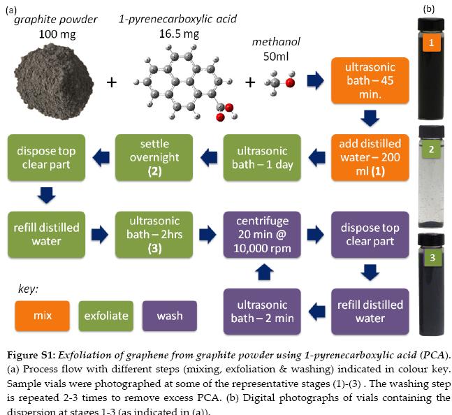
"There are high-throughput methods for making graphene oxide, which is not as conductive as graphene, and there are low-throughput methods for making pure graphene," said lead co-author Matteo Pasquali, professor of chemical and biomolecular engineering and chemistry at Rice. "Our method yields very pure material, and it is based on bulk fluid-processing techniques that have long been used by the chemical industry."

Pasquali said the research team found it could dissolve graphite in chlorosulphonic acid, a common industrial solvent. The researchers had to devise new methods to measure the aggregation of the dissolved graphene flakes, but at the end the team was pleasantly surprised to find that the individual graphene layers in the graphite peeled apart spontaneously. The team was able to dissolve as much as two grams of graphene per liter of acid to produce solutions at least 10 times more concentrated than existing methods.

The researchers took advantage of novel cryogenic techniques for electron microscopy that allowed them to directly image the graphene sheets in the chlorosulfonic acid.

"We applied new methods that we had developed to directly image carbon nanotubes in acid," said co-author Yeshayahu "Ishi" Talmon, professor of chemical engineering at the Technion-Israel Institute of Technology. "This was no small feat considering the nature of the acid and the difficulty of specimen preparation and imaging."

Using the concentrated solutions of dissolved graphene, the scientists made transparent films that were electrically conductive. Such films could be useful in making touch screens that are less expensive than those used in today's smart phones. In addition, the researchers also produced liquid crystals.

"If you can make liquid crystals, you can spin fibers," said study co-author James Tour, Rice's T.T. and W.F. Chao Professor of Chemistry. "In liquid crystals, the individual sheets align themselves into domains, and having some measure of alignment allows you to flow the material through narrow openings to create fibers."

If the method proves useful for making graphene fibers in bulk, it could drive down the cost of the ultrastrong carbon composites used in the aerospace, automotive and construction industries.

The research was funded by the Air Force Office of Scientific Research, the Department of Energy, the Air Force Research Laboratory, the Welch Foundation, the U.S. Army Corps of Engineers and the USA-Israel Binational Science Foundation. Co-authors include Natnael Behabtu, Jay Lomeda, Micah Green, Amanda Higgenbotham, Alexander Sinitskii, Dmitry Kosynkin, Dmitri Tsentalovich and Nicholas Parra-Vasquez, all of Rice's Smalley Institute for Nanoscale Science and Technology; and Judith Schmidt, Ellina Kesselman and Yachin Cohen, all of the Technion-Israel Institute of Technology.

#190 valkyrie_ice

  • Topic Starter
  • Guest
  • 837 posts
  • 142
  • Location:Monteagle, TN

Posted 07 June 2010 - 12:48 AM

Thank You Niner. That was indeed an important development, and you posted it just hours prior to my reading it elsewhere.

And another interesting development:

http://www.engadget....irtual-pottery/

Want to reenact Ghost but don't care for all the messy bits? Let lasers do the work for you. L'Artisan Electronique uses a laser scanner to detect your hand-sculpting gestures, transfers their gently urging instructions over to a computerized 3D model, and -- should your production exhibit sufficient creativity or je ne sais quoi -- prints it out using a 3D ceramic printer. This is part of a Design by Performance exhibition taking place over in Belgium and is seriously one of the cooler things you're going to come across today -- or any other day, for that matter.


View on Vimeo.


High level design tools used to create low level products. Sculpt a virtual object to create a real one. Play around endlessly before finalizing and making the "hard copy"

Yet one more step towards DMUs.

Edited by valkyrie_ice, 07 June 2010 - 12:50 AM.


#191 valkyrie_ice

  • Topic Starter
  • Guest
  • 837 posts
  • 142
  • Location:Monteagle, TN

Posted 07 June 2010 - 06:33 PM

And more interesting news:

http://nextbigfuture...onto-pills.html

Researchers at the University of Leeds, Durham University, and GlaxoSmithKline have teamed up to create pills that can be printed.

* 99.9 percent of a pill is filler

* Printing pills means literally printing the active ingredients of a medication onto the side of a tablet. To understand the concept of "printing," think of the active ingredients as tiny droplets that can be printed onto a surface the way ink is printed onto paper, but instead of paper, it's a tablet. That means pills could be individually made for each patient to fit their medical needs and one pill could potentially hold more than one type of medication.


a medical DMU.


And in the field of AI: http://nextbigfuture...f-lifelike.html

The article cover multiple topics so I recommend simply following the link and reading.

#192 niner

  • Guest
  • 16,276 posts
  • 2,000
  • Location:Philadelphia

Posted 07 June 2010 - 09:18 PM

Researchers at the University of Leeds, Durham University, and GlaxoSmithKline have teamed up to create pills that can be printed.

* 99.9 percent of a pill is filler

* Printing pills means literally printing the active ingredients of a medication onto the side of a tablet.

This will only work for drugs that are used in very small quantities. If you need 100 mg of the active compound, then you will need to use a more conventional formulation. Good for LSD, and maybe LDN, but not for Ibuprofen. It's still a cool application, and might indeed be useful for pharmacogenomic customization.

#193 valkyrie_ice

  • Topic Starter
  • Guest
  • 837 posts
  • 142
  • Location:Monteagle, TN

Posted 08 June 2010 - 04:44 PM

Researchers at the University of Leeds, Durham University, and GlaxoSmithKline have teamed up to create pills that can be printed.

* 99.9 percent of a pill is filler

* Printing pills means literally printing the active ingredients of a medication onto the side of a tablet.

This will only work for drugs that are used in very small quantities. If you need 100 mg of the active compound, then you will need to use a more conventional formulation. Good for LSD, and maybe LDN, but not for Ibuprofen. It's still a cool application, and might indeed be useful for pharmacogenomic customization.


Thats right now. Where it will be in five years could be a entirely different story. There will be improvements made I am sure, especially as we are developing more sophisticated molecular medicines.

a little bit more on the Graphene story you linked:

The Rice researchers recently demonstrated that even stronger superacids can separate graphite into sheets of graphene and bring them into solution. Unlike other methods involving chemical reactions that alter graphene, the superacid solution does not degrade the material's properties. The group has used the solutions to make sheets of graphene with low electrical resistance and is now "full steam ahead" using these solutions to make graphene fibers, says Tour.

Tour expects the graphene processing method to have two major applications: transparent electrodes and structural materials. In both areas, it may bring down costs. Indium tin oxide, the transparent conducting material most commonly found in touch screens and solar cells, is expensive and brittle, says Benji Maruyama, senior materials research engineer at the Air Force Research Laboratory in Ohio. The U.S. Air Force is funding the Rice research. Many groups have demonstrated the advantages of graphene electrodes in terms of conductivity and flexibility; the Rice method should make it possible to manufacture them over large areas.


With the news earlier about graphane (graphene with a layer of hydrogen coating both sides) being usable for making quantum wells, this is starting to look more and more as if graphene could be used to make ultralightweight multifunctional electronics. i.e. A display which is also a computer, touchscreen, camera, and smartphone, but which is as thin as a credit card, solar powered, flexible, and has no moving parts. With printing technology, it might even be so cheap it's "disposable"

The "smartVRphone" of the future is looking like it might be 100% carbon.

#194 valkyrie_ice

  • Topic Starter
  • Guest
  • 837 posts
  • 142
  • Location:Monteagle, TN

Posted 08 June 2010 - 05:36 PM

From IEET

Free book on automation and structural unemployment

Posted: Jun 2, 2010

Martin Ford and his publishers have decided to make the PDF version of his The Lights in the Tunnel free to download and free to share.

Please feel free to forward this to anyone who might be interested and/or post it for download.

The free PDF can also be downloaded directly from http://www.thelightsinthetunnel.com.


Also available here: http://ieet.org/arch...IGHTSTUNNEL.PDF

from the web blurb:

What will the economy of the future look like?

Where will advancing technology, job automation, outsourcing and globalization lead?

Is it possible that accelerating computer technology was a primary cause of the current global economic crisis—and that even more disruptive impacts lie ahead?

This groundbreaking book by a Silicon Valley computer engineer and entrepreneur explores these questions and shows how accelerating technology is likely to have a highly disruptive influence on our economy in the near future—and may well already be a significant factor in the current global crisis.

THE LIGHTS IN THE TUNNEL employs a powerful thought experiment to explore the economy of the future. An imaginary "tunnel of lights" is used to visualize the economic implications of the new technologies that are likely to appear in the coming years and decades.

The book directly challenges nearly all conventional views of the future and illuminates the danger that lies ahead if we do not plan for the impact of rapidly advancing technology. It also offers unique insights into how technology will intertwine with globalization to shape the twenty-first century and explores ways in which the economic realities of the future might be leveraged to drive prosperity and to address global challenges such as poverty and climate change.


Just started reading.

Edited by valkyrie_ice, 08 June 2010 - 05:38 PM.


#195 Reno

  • Guest
  • 584 posts
  • 37
  • Location:Somewhere

Posted 09 June 2010 - 02:09 PM

Is it just me or has there been less and less nanotechnology research news lately?

#196 valkyrie_ice

  • Topic Starter
  • Guest
  • 837 posts
  • 142
  • Location:Monteagle, TN

Posted 09 June 2010 - 04:39 PM

Is it just me or has there been less and less nanotechnology research news lately?


I've seen less RESEARCH, and a lot more Engineering lately. It's been moving out of theory into prototypes, and not all "Nano" per se, as a lot of it is now "Bio" or "Electronics"

#197 valkyrie_ice

  • Topic Starter
  • Guest
  • 837 posts
  • 142
  • Location:Monteagle, TN

Posted 11 June 2010 - 05:20 AM

And in Graphene news, from Science Daily:

http://www.scienceda...00610141036.htm

ScienceDaily (June 10, 2010) — Scientists have made a breakthrough toward creating nanocircuitry on graphene, widely regarded as the most promising candidate to replace silicon as the building block of transistors. They have devised a simple and quick one-step process based on thermochemical nanolithography (TCNL) for creating nanowires, tuning the electronic properties of reduced graphene oxide on the nanoscale and thereby allowing it to switch from being an insulating material to a conducting material.

The technique works with multiple forms of graphene and is poised to become an important finding for the development of graphene electronics. The research appears in the June 11, 2010, issue of the journal Science.

Scientists who work with nanocircuits are enthusiastic about graphene because electrons meet with less resistance when they travel along graphene compared to silicon and because today's silicon transistors are nearly as small as allowed by the laws of physics. Graphene also has the edge due to its thickness -- it's a carbon sheet that is a single atom thick. While graphene nanoelectronics could be faster and consume less power than silicon, no one knew how to produce graphene nanostructures on such a reproducible or scalable method. That is until now.

"We've shown that by locally heating insulating graphene oxide, both the flakes and epitaxial varieties, with an atomic force microscope tip, we can write nanowires with dimensions down to 12 nanometers. And we can tune their electronic properties to be up to four orders of magnitude more conductive. We've seen no sign of tip wear or sample tearing," said Elisa Riedo, associate professor in the School of Physics at the Georgia Institute of Technology.


In other words, they have now figured out how to directly write graphene circuits. While this is a slow process compared to chip at once printing, it means we can make precise, replicatable devices on the 12 nanometer scale, which should allow much faster development in graphene electronics.

#198 valkyrie_ice

  • Topic Starter
  • Guest
  • 837 posts
  • 142
  • Location:Monteagle, TN

Posted 21 June 2010 - 07:54 PM

http://www.physorg.c...s196316695.html


(PhysOrg.com) -- Graphene is a relatively new material with outstanding electrical, chemical and mechanical properties that make it an attractive material for use as flexible conductors of the sort used in gadgets such as touch screens and flat panel TVs. In the past attempts to make large films of graphene have been unsuccessful, but now a team of scientists from South Korea and Japan have succeeded in roll-to-roll production of graphene films, growing them by chemical vapor deposition onto flexible copper substrates.

Graphene is composed of a single layer of carbon atoms in a honeycomb- shaped lattice. It was first isolated in 2004. The material is highly conductive, extremely strong, and is almost transparent, which makes it ideal for high-speed electronic devices.

The researchers grew their graphene sheets by chemical vapor depositiononto large sheets of copper foil. They coated the graphene with a thin layer of adhesive polymer and then dissolved away the copper backing. Using rollers, the graphene was then pressed against another substrate, such as PET, and the polymer layer was removed by heating, leaving a film of graphene. They repeated the process to produce a sheet of four layers of graphene on top of each other. This four-layer sheet was then treated with nitric acid to improve its electrical conductivity.

The rectangular sheets, which measured 76 cm on the diagonal, were of extremely high quality, with the four-layer stack of films exhibiting superior electrical resistance to commercially available transparent electrodes such as indium tin oxides (ITO). The films were almost transparent, allowing 90% of light to pass through.


Two things to note here. Large scale "printing" of graphene sheets using Roll to Roll printing presses and Chemical Vapor deposition. And second, that graphene circuits can be 90% transparent, and this is PRIOR to actual nanoribbon based graphene circuits.

One more step towards those VR lenses I've been talking about.

#199 Reno

  • Guest
  • 584 posts
  • 37
  • Location:Somewhere

Posted 21 June 2010 - 08:16 PM

That's fantastic news there. That was one of the main hurdles keeping them from using graphine in hardware mass production. It'll be nice to have my computer go 1000ghz in a few years.

Hey valkyrie girl, when you post one of these news articles in here for discussion, can you post a copy in the other info threads? That way there is one place for CNT news, graphine, cancer etc. It makes it easier for me to find particular articles.

Edited by Reno, 21 June 2010 - 08:16 PM.


#200 valkyrie_ice

  • Topic Starter
  • Guest
  • 837 posts
  • 142
  • Location:Monteagle, TN

Posted 21 June 2010 - 09:52 PM

That's fantastic news there. That was one of the main hurdles keeping them from using graphine in hardware mass production. It'll be nice to have my computer go 1000ghz in a few years.

Hey valkyrie girl, when you post one of these news articles in here for discussion, can you post a copy in the other info threads? That way there is one place for CNT news, graphine, cancer etc. It makes it easier for me to find particular articles.


Certainly. I tend to post articles I see as stepping stones to the next phase, so it's a bit disjointed. Reposting them in categories will certainly help to keep them organized for those looking for just the news Posted Image

Edited by valkyrie_ice, 21 June 2010 - 09:53 PM.


#201 valkyrie_ice

  • Topic Starter
  • Guest
  • 837 posts
  • 142
  • Location:Monteagle, TN

Posted 22 June 2010 - 03:51 AM

Posted Image
Posted Image
Posted Image
I ran into this while randomly following links.

If you are not a anime fan, it's Saber from Fate/Stay Night. Or rather a Cosplayer in a new style of full mask costume.

Why do I post it here? Because it's another case of a virtual character in the real world. We don't even yet have VR, and already we are making efforts to make it possible for someone to look EXACTLY like a virtual character.

And in this case, Fate/Stay Night started as a Interactive Visual Novel, before it became an anime and a Manga.

#202 Reno

  • Guest
  • 584 posts
  • 37
  • Location:Somewhere

Posted 22 June 2010 - 05:54 AM

I can't say I really understand the draw of VR. I'd more rather be it then dream it. Sure VR will be a precursor to true molecular nanotech, but not by some enormous amount of time. If Kurzweil is right then all those people who measure progress by today's static standards, and not a dynamic rate of change are in for a surprise. Call me an optimist but I believe Ray when he says true molecular nanotechnology is but ~twenty years away.

#203 valkyrie_ice

  • Topic Starter
  • Guest
  • 837 posts
  • 142
  • Location:Monteagle, TN

Posted 22 June 2010 - 06:04 AM

I can't say I really understand the draw of VR. I'd more rather be it then dream it. Sure VR will be a precursor to true molecular nanotech, but not by some enormous amount of time. If Kurzweil is right then all those people who measure progress by today's static standards, and not a dynamic rate of change are in for a surprise. Call me an optimist but I believe Ray when he says true molecular nanotechnology is but ~twenty years away.


I'm looking at basic morphological freedom in less than that. check out my reply in http://www.imminst.o...ndpost&p=414486

With the speed with which we are developing in just the last two years, I think basic 1st gen nanotech is only about 10 years away, and 2nd gen maybe five more after that.


And that "I'd rather BE it than Dream it" is precisely why I say VR will be little more than a stepping stone to making what VR can provide a reality outside VR.

Which is what the pic of Saber is about. Making a VR reality REAL reality.

Edited by valkyrie_ice, 22 June 2010 - 06:07 AM.


#204 Luna

  • Guest, F@H
  • 2,528 posts
  • 66
  • Location:Israel

Posted 22 June 2010 - 12:28 PM

Cool! and pretty :)

But impractical for wearing a whole day + regarded as weird + not really you (and you will feel it).

#205 Elus

  • Guest
  • 793 posts
  • 723
  • Location:Interdimensional Space

Posted 22 June 2010 - 06:58 PM


World's First Plastic Antibodies in Live Organisms: Stop Spread of Bee Venom in Mice


UC Irvine researchers have developed the first "plastic antibodies" successfully employed in live organisms -- stopping the spread of bee venom through the bloodstream of mice.

[Link] http://www.scienceda...00621141026.htm


#206 valkyrie_ice

  • Topic Starter
  • Guest
  • 837 posts
  • 142
  • Location:Monteagle, TN

Posted 22 June 2010 - 07:35 PM

Cool! and pretty :)

But impractical for wearing a whole day + regarded as weird + not really you (and you will feel it).


It's not the costume that's the point dear. It's the effort that went into making a virtual character into a REAL LIFE one. The same effort that will go into creating medical technologies to enable morphological freedom as well.

And weirdness is a temporary phenomena. It's novelty wears off and becomes just ordinary as it becomes more common.
And to Elus, I did see that earlier, about the use of completely artificial antibodies undergoing tests. Very neat stuff.

And to Reno, I was re-reading that last news post and actually paid attention to what they made. It was a touchscreen. 2x as tough as the current touchscreen tech, uses no rare earth elements, and the copper that they form the original CVD layers on is 100% recycled. That has some very immediate possible uses, particularly when you put it together with an article I read on Physorg about graphene OLED displays http://www.physorg.c...s187430392.html

Researchers at Stanford University have successfully developed brand new concept of organic lighting-emitting diodes (OLEDs) with a few nanometer of graphene as transparent conductor. This paved the way for inexpensive mass production of OLEDs on large-area low-cost flexible plastic substrate, which could be rolled up like wallpaper and virtually applied to anywhere you want.

Due to its superb image quality, low power consumption and ultra-thin device structure, OLED has been developed for more than 20 years, and recently finds its application in ultra-thin televisions and other display screens such as those on digital cameras and mobile phones. OLEDs consist of active organic luminescent structure sandwiched between two electrodes, one of which must be transparent. Traditionally, indium tin oxide (ITO) is used in this type of devices. However, indium is rare, expensive and difficult to recycle. Scientists have been actively searching for an alternative candidate.

The next generation of optoelectronic devices requires transparent conductive electrodes to be lightweight, flexible, cheap, environmental attractive, and compatible with large-scale manufacturing methods. Graphene, single layer of graphite, is becoming a very promising candidate due to its unique electrical and optical properties in last two years. Very recently, Junbo Wu et al., researchers at Stanford University, successfully demonstrated the application of graphene in OLEDs for the first time.


Put those two articles together and what you have is Video Wallpaper that has touchscreen controls. Which can be printed on a LOT more than just plastic. We may be seeing some very impressive display technology coming not only to our walls, but to our clothes our cars, and of course, our cereal boxes.

Oh, and California is debating about replacing License plates with OLED displays http://blogs.forbes....license-plates/ Why? Creative revenue creation.


#207 valkyrie_ice

  • Topic Starter
  • Guest
  • 837 posts
  • 142
  • Location:Monteagle, TN

Posted 22 June 2010 - 08:03 PM

And more graphene news:

http://nextbigfuture...ne-25-inch.html

Researchers have created a flexible graphene sheet with silver electrodes printed on it (top) that can be used as a touch screen when connected to control software on a computer (bottom). Credit: Byung Hee Hong, SKKU. 2. Researchers at Samsung and Sungkyunkwan University, in Korea, have produced a continuous layer of pure graphene the size of a large television, spooling it out through rollers on top of a flexible, see-through, 63-centimeter-wide (25 inch) polyester sheet.

The team has already created a flexible touch screen by using the polymer-supported graphene to make the screen's transparent electrodes. The material currently used to make transparent electronics, indium tin oxide, is expensive and brittle. Producing graphene on polyester sheets that bend is the first step to making transparent electronics that are stronger, cheaper, and more flexible. "You could theoretically roll up your iPhone and stick it behind your ear like a pencil," says Tour


It links to http://www.technolog...ting/25633/?a=f which gives a little more detail than the Physorg peice.But this NBF story also covers this little tidbit as well:


Researchers at Rensselaer Polytechnic Institute have developed a simple new method for producing large quantities of the promising nanomaterial graphene. The new technique works at room temperature, needs little processing, and paves the way for cost-effective mass production of graphene.

Posted Image

By submerging graphite in a mixture of dilute organic acid, alcohol, and water, and then exposing it to ultrasonic sound, the team discovered that the acid works as a "molecular wedge, " which separates sheets of graphene from the parent graphite. The process results in the creation of large quantities of undamaged, high-quality graphene dispersed in water. Kar and team then used the graphene to build chemical sensors and ultracapacitors

We present a scalable and facile technique for noncovalent functionalization of graphene with 1-pyrenecarboxylic acid that exfoliates single-, few-, and multilayered graphene flakes into stable aqueous dispersions. The exfoliation mechanism is established using stringent control experiments and detailed characterization steps. Using the exfoliated graphene, we demonstrate highly sensitive and selective conductometric sensors (whose resistance rapidly changes >10000% in saturated ethanol vapor), and ultracapacitors with extremely high specific capacitance (120 F/g), power density (105 kW/kg), and energy density (9.2 Wh/kg).


http://news.rpi.edu/...tcenterkey=2742

http://pubs.acs.org/....1021/nl903557p

Those last two links are about the second story.
  • like x 1

#208 valkyrie_ice

  • Topic Starter
  • Guest
  • 837 posts
  • 142
  • Location:Monteagle, TN

Posted 23 June 2010 - 05:28 PM

And for those who keep saying Nanotech is decades away, I really have to wonder how you can possibly think that when News like THIS: http://www.scienceda...00622091740.htm keeps popping up on a regular basis.

By emulating nature's design principles, a team at Harvard's Wyss Institute for Biologically Inspired Engineering, Harvard Medical School and Dana-Farber Cancer Institute has created nanodevices made of DNA that self-assemble and can be programmed to move and change shape on demand. In contrast to existing nanotechnologies, these programmable nanodevices are highly suitable for medical applications because DNA is both biocompatible and biodegradable.

The work appears in the June 20 advance online Nature Nanotechnology.

Built at the scale of one billionth of a meter, each device is made of a circular, single-stranded DNA molecule that, once it has been mixed together with many short pieces of complementary DNA, self-assembles into a predetermined 3D structure. Double helices fold up into larger, rigid linear struts that connect by intervening single-stranded DNA. These single strands of DNA pull the struts up into a 3D form -- much like tethers pull tent poles up to form a tent. The structure's strength and stability result from the way it distributes and balances the counteracting forces of tension and compression.

This architectural principle -- known as tensegrity -- has been the focus of artists and architects for many years, but it also exists throughout nature. In the human body, for example, bones serve as compression struts, with muscles, tendons and ligaments acting as tension bearers that enable us to stand up against gravity. The same principle governs how cells control their shape at the microscale.

"This new self-assembly based nanofabrication technology could lead to nanoscale medical devices and drug delivery systems, such as virus mimics that introduce drugs directly into diseased cells," said co-investigator and Wyss Institute director Don Ingber. A nanodevice that can spring open in response to a chemical or mechanical signal could ensure that drugs not only arrive at the intended target but are also released when and where desired.

Further, nanoscopic tensegrity devices could one day reprogram human stem cells to regenerate injured organs. Stem cells respond differently depending on the forces around them. For instance, a stiff extracellular matrix -- the biological glue surrounding cells -- fabricated to mimic the consistency of bone signals stem cells to become bone, while a soupy matrix closer to the consistency of brain tissue signals the growth of neurons. Tensegrity nanodevices "might help us to tune and change the stiffness of extracellular matrices in tissue engineering someday," said first author Tim Liedl, who is now a professor at Ludwig-Maximilians-Universität in Munich.

"These little Swiss Army knives can help us make all kinds of things that could be useful for advanced drug delivery and regenerative medicine," said lead investigator William Shih, Wyss core faculty member and associate professor of biological chemistry and molecular pharmacology at HMS and Dana-Farber Cancer Institute. "We also have a handy biological DNA Xerox machine that nature evolved for us," making these devices easy to manufacture.


It's not even mid year, and this is something along the lines of the thirtieth major nanotech breakthrough this year alone?


And Reno and Luna, if you read my link above to my comments about programmable Stem Cells being used as natural medical nanobots, you can see yet another piece of the puzzle being put into place here.

I can't wait to see what the next half year brings

Posted Image


  • like x 1

#209 valkyrie_ice

  • Topic Starter
  • Guest
  • 837 posts
  • 142
  • Location:Monteagle, TN

Posted 24 June 2010 - 11:05 PM

You should find this interesting Reno. Looks like DARPA is taking the promises of graphene extremely seriously.

http://nextbigfuture...vances-for.html

DARPA describes its Ubiquitous High Performance Computing (UHPC) - 70 pages
Yes, it would exaflop supercomputers on the supercomputer end but it would also mean superfast and robust future smartphones. It will mean selfware operating systems and more hack resistent computers and networks.

The UHPC program will develop the architectures and technologies that will provide the framework and underpinnings for the resolution of the power consumption, cyber resiliency, and productivity problems. The UHPC program will develop computer systems, from the embedded to cabinet system levels, that have extremely high-energy efficiency. These systems will have dramatically reduced power consumption while delivering a thousand fold increases in capabilities.

The UHPC vision includes:

• Efficiency: New system-wide (hardware and software) technology approaches to minimize energy dissipation per operation and maximize energy efficiency, without sacrificing scalability to ultra-high performance DoD applications.
• Programmability: Develop new scalable system architectures and technologies that do not require application programmers to explicitly manage system complexity, in terms of architectural attributes with respect to data locality and concurrency, to achieve performance, time to solution and other goals.
• Dependability: Develop a system-wide approach to achieve dependability through fault management techniques enabling an application to execute correctly through both failures and attacks, and to protect the confidentiality and integrity of information, while achieving the user's goals. These goals could include performance, time to solution, energy efficiency or power consumption. Dependability across all levels of a UHPC System Design that is nearly transparent to the user and hardware performance.
* To realize this vision requires reinventing how computers process and manage data and how applications are developed and executed. UHPC System Designs that merely pursue evolutionary development will not be considered.

To reach the energy goals alone will require reducing energy per operation from thousands of pJ/Op (representative of current processors), to tens of pJ/Op. As an example, achieving 50 GFLOPS/W is equivalent to expending only 20 pJ per floating point operation – a budget that must encompass far more than just the floating point operation: leakage losses, operand accesses, and operand transport, along with instruction issue and concurrency control. This will require energy-optimized solutions from the basic functional elements through subsystems and systems


UHPC Goals

The goals of the UHPC program are as follows:
• Single cabinet system that achieves the UHPC program vision and goals. The hardware system goals areas described in the document.
• Self-aware OS and the resulting new system software stack. • Prototype compiler for the new programming model, that enables ease of programming for an ExtremeScale system.
• Dynamic system that adapts to achieve optimal application execution goals, without the direct involvement of the application developer.
• UHPC System Design that supports modern high performance for scientific and engineering applications.
• UHPC System Design based on a multi-level model of dependability.
• Processor module that is capable of being used within terascale embedded and multiple cabinet systems.
• Development efforts must utilize open innovation and software and hardware co-design throughout the life of the program.

Posted Image


The UHPC software effort spans operating systems; runtime systems for scheduling and lower level resource management; memory management; communication; performance monitoring; power management; self-aware operation; and prototype compilers. It is anticipated that a new system software stack will be developed for a UHPC System. The UHPC program will not provide funding for research and development of large-scale parallel file systems, high bandwidth I/O and storage technologies. However, it is a requirement that a UHPC System include these components.


UHPC Challenge Problems

There are five UHPC Challenge Problems:
• Massive streaming sensor data problem resulting in actionable knowledge,
• Large dynamic graph-based informatics problem,
• Decision class problem that encompasses search, hypothesis testing, and planning,
• Two challenge problems drawn from DoD applications and to be selected after UHPC program initiation.

Initial primary metrics
Metrics that will be used through the life of the program are:
• Energy efficiency: 50 GFLOPS/W for the HPL benchmark
• System Performance: 1 PFLOPS for the HPL benchmark
• Programmability: TBD
• Dependability: TBD
• Cabinet Power Requirement

Posted Image


The two phases covered under this solicitation will have period of performances and funding splits as follows;

Phase 1 will be 24 months:
• Each TA1 team receiving up to 3.25 million US dollars the first year and up to 5.25 million dollars the second year;
• One TA2 team receiving up to 1.75 million US dollars each year;

Phase 2 will be 24 months long:
• Each TA1 team receiving up to 8.65 million US dollars per 12 month period;
• One TA2 team receiving up to 2 million US dollars per 12 month period;


  • like x 1

#210 niner

  • Guest
  • 16,276 posts
  • 2,000
  • Location:Philadelphia

Posted 25 June 2010 - 04:41 AM

• Self-aware OS and the resulting new system software stack.

That sounds interesting...

they forgot:
• Must run Vista without crashing too much.


0 user(s) are reading this topic

0 members, 0 guests, 0 anonymous users