• Log in with Facebook Log in with Twitter Log In with Google      Sign In    
  • Create Account
  LongeCity
              Advocacy & Research for Unlimited Lifespans


Adverts help to support the work of this non-profit organisation. To go ad-free join as a Member.


Photo
* * * * * 3 votes

Carbon Nanotube Thread


  • Please log in to reply
37 replies to this topic

#1 Reno

  • Guest
  • 584 posts
  • 37
  • Location:Somewhere

Posted 12 January 2009 - 09:41 PM


Instead of making a new thread for every nanotube news article I'm just going to post them here.


Posted Image Posted Image

Definition from Wikipedia

Carbon nanotubes (CNTs) are allotropes of carbon with a nanostructure that can have a length-to-diameter ratio greater than 10,000,000 and as high as 40,000,000 as of 2004. These cylindrical carbon molecules have novel properties that make them potentially useful in many applications in nanotechnology, electronics, optics and other fields of materials science, as well as potential uses in architectural fields. They exhibit extraordinary strength and unique electrical properties, and are efficient conductors of heat. Their final usage, however, may be limited by their potential toxicity.

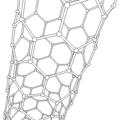
Nanotubes are members of the fullerene structural family, which also includes the spherical buckyballs. The cylindrical nanotube usually has at least one end capped with a hemisphere of the buckyball structure. Their name is derived from their size, since the diameter of a nanotube is in the order of a few nanometers (approximately 1/50,000th of the width of a human hair), while they can be up to several millimeters in length (as of 2008). Nanotubes are categorized as single-walled nanotubes (SWNTs) and multi-walled nanotubes (MWNTs).

The nature of the bonding of a nanotube is described by applied quantum chemistry, specifically, orbital hybridization. The chemical bonding of nanotubes is composed entirely of sp2 bonds, similar to those of graphite. This bonding structure, which is stronger than the sp3 bonds found in diamonds, provides the molecules with their unique strength. Nanotubes naturally align themselves into "ropes" held together by Van der Waals forces. Under high pressure, nanotubes can merge together, trading some sp² bonds for sp³ bonds, giving the possibility of producing strong, unlimited-length wires through high-pressure nanotube linking.


Edited by bobscrachy, 12 January 2009 - 09:48 PM.

  • like x 1

#2 Reno

  • Topic Starter
  • Guest
  • 584 posts
  • 37
  • Location:Somewhere

Posted 12 January 2009 - 09:45 PM

A Better Way to Make Nanotubes

A compound synthesized for the first time by Berkeley Lab scientists could help to push nanotechnology out of the lab and into faster electronic devices, more powerful sensors, and other advanced technologies.

The scientists developed a hoop-shaped chain of benzene molecules that had eluded synthesis, despite numerous efforts, since it was theorized more than 70 years ago.

The much-anticipated debut of the compound, called cycloparaphenylene, couldn’t be better timed. It comes as scientists are working to improve the way carbon nanotubes are produced, and the newly synthesized nanohoop happens to be the shortest segment of a carbon nanotube. Scientists could use the segment to grow much longer carbon nanotubes in a controlled way, with each nanotube identical to the next.

“The holy grail in this field is to come up with a way to make a single type of carbon nanotube on demand,” says Ramesh Jasti, a postdoctoral researcher in Berkeley Lab’s Materials Sciences Division. “And this compound moves us toward this goal of rational synthesis.”

Jasti conducted the research at the Molecular Foundry, a U.S. Department of Energy User Facility located at Berkeley Lab that provides support to nanoscience researchers around the world. He worked with Carolyn Bertozzi, director of the Molecular Foundry, as well as other Berkeley Lab scientists.

To synthesize the elusive cycloparaphenylene, the team developed a relatively simple, low-temperature way to bend a string of benzene rings — which normally resist bending — into a hoop. The result is a structure that is as unusual as it is potentially useful. It should be flat, but it’s circular. And it’s poised to improve the way one of most promising stars in nanotechnology is produced.

Carbon nanotubes are hollow wires of pure carbon about 50,000 times narrower than a human hair. They can be semiconducting or metallic depending on how they’re structured. Their unique properties could usher in a new era of faster and smaller computers, or tiny sensors powerful enough to detect a single molecule.

But carbon nanotubes haven’t made inroads into the electronics industry and other sectors because they’re difficult to make in large quantities. They’re currently produced in batches, with only a handful of nanotubes in each batch possessing the desired characteristics. This shotgun approach works fine in the lab, but it’s too inefficient for commercial applications.

Cycloparaphenylene offers a more targeted approach. The family of compounds forms the smallest carbon hoop structure with a set diameter and set orientation of benzene molecules, which are the two variables that determine a nanotube’s electronic properties. Because of this, cycloparaphenylene molecules could be used as seeds or templates to grow large batches of carbon nanotubes with just the right specifications.

This combination of precision and high yield will be needed if carbon nanotubes are to make the jump from the lab to the commercial sector. In order for carbon nanotubes to replace silicon wafers in electronics, for example, they’ll need to be just as unblemished as silicon wafers, and just as easy to make in large numbers.

“This compound, which we synthesized for the first time, could help us create a batch of carbon nanotubes that is 99 percent of what we want, rather than fish out the one percent like we do today,” says Jasti. “The idea is to take the smallest fragment of a carbon nanotube, and use that to build tubular structures.”

The research, which is published in a recent issue of the Journal of the American Chemical Society, was funded in part by the Department of Energy.


source

#3 Reno

  • Topic Starter
  • Guest
  • 584 posts
  • 37
  • Location:Somewhere

Posted 19 January 2009 - 08:59 PM

Swallowing a nanotechnology pill based on carbon nanotubes.

Article here ------> Read this

sponsored ad

  • Advert

#4 Cyberbrain

  • Guest, F@H
  • 1,755 posts
  • 2
  • Location:Thessaloniki, Greece

Posted 19 January 2009 - 09:14 PM

Posted Image
Four scanning electron microscope images of the spinning of carbon nanotube fibres.

Posted Image
Top: An optical image of the interdigitated gold electrodes upon which the carbon nanotubes are deposited. Bottom: A scanning electron microscopy image of the gold electrodes (thick gray bars). The carbon nanotubes are the small string-like wires extending into the black regions between the electrodes. Using carbon nanotubes, MIT chemical engineers have built the most sensitive electronic detector yet for sensing deadly gases such as the nerve agent sarin. The technology, which could also detect mustard gas, ammonia and VX nerve agents, has potential to be used as a low-cost, low-energy device that could be carried in a pocket or deployed inside a building to monitor hazardous chemicals. Link

Posted Image
Types of Carbon Nanotubes.

#5 Reno

  • Topic Starter
  • Guest
  • 584 posts
  • 37
  • Location:Somewhere

Posted 27 January 2009 - 03:24 PM

Long, Stretchy Carbon Nanotubes Could Make Space Elevators Possible

Scientists from Cambridge University have developed a light, flexible, and strong type of carbon nanotube material that may bring space elevators closer to reality. Motivated by a $4 million prize from NASA, the scientists found a way to combine multiple separate nanotubes together to form long strands. Until now, carbon nanotubes have been too brittle to be formed into such long pieces.

And a space elevator - if it ever becomes reality - will be quite long. NASA needs about 144,000 miles of nanotube to build one. In theory, a cable would extend 22,000 miles above the Earth to a station, which is the distance at which satellites remain in geostationary orbit. Due to the competing forces of the Earth's gravity and outward centrifugal pull, the elevator station would remain at that distance like a satellite. Then the cable would extend another 40,000 miles into space to a weighted structure for stability. An elevator car would be attached to the nanotube cable and powered into space along the track.

NASA and its partner, the Spaceward Foundation, hope that a space elevator could serve as a cost-effective and relatively clean mode of space transportation. NASA's current shuttle fleet is set to retire in 2010, and the organization doesn't have enough funds to replace it until 2014 at the earliest. To fill the gap, NASA is hiring out shuttles to provide transportation to the International Space Station from private companies.

So NASA could use a space elevator, the sooner the better. Space elevators could lift material at just one-fifth the cost of a rocket, since most of a rocket's energy is used simply to escape Earth's gravity. Not only could a space elevator offer research expeditions for astronauts, the technology could also expand the possibilities for space tourism and even space colonization.

Currently, the Cambridge team can make about 1 gram of the new carbon material per day, which can stretch to 18 miles in length. Alan Windle, professor of materials science at Cambridge, says that industrial-level production would be required to manufacture NASA's request for 144,000 miles of nanotube. Nevertheless, the web-like nanotube material is promising.

"The key thing is that the process essentially makes carbon into smoke, but because the smoke particles are long thin nanotubes, they entangle and hold hands," Windle said. "We are actually making elastic smoke, which we can then wind up into a fiber."

Windle and his colleagues presented their results last month at a conference in Luxembourg, which attracted hundreds of attendees from groups such as NASA and the European Space Agency. John Winter of EuroSpaceward, which organized the conference, thought the new material was a significant step.

"The biggest problem has always been finding a material that is strong enough and lightweight enough to stretch tens of thousands of miles into space," said Winter. "This isn't going to happen probably for the next decade at least, but in theory this is now possible. The advances in materials for the tether are very exciting."


source

#6 Cyberbrain

  • Guest, F@H
  • 1,755 posts
  • 2
  • Location:Thessaloniki, Greece

Posted 27 January 2009 - 03:51 PM

Long, Stretchy Carbon Nanotubes Could Make Space Elevators Possible

source

This is one of my largest hopes for carbon nanotubes.

#7 Futurist1000

  • Guest
  • 438 posts
  • 1
  • Location:U.S.A.

Posted 30 January 2009 - 03:20 AM

Here's some information about researchers who are developing artificial neurons synthesized with carbon nanotubes.

Synthetic brains are a long way from reality, but researchers at the University of Southern California, funded by the National Science Foundation, are taking the first steps to build neurons from carbon nanotubes that emulate human brain function "At this point we still don't know if building a synthetic brain is feasible," said Alice Parker, professor of electrical engineering. "It may take decades to realize anything close to the human brain but emulating pieces of the brain, such as a synthetic vision system or synthetic cochlea that interface successfully with a real brain may be available quite soon, and synthetic parts of the brain's cortex within decades."

The researchers have shown that portions of a neuron can be modeled electronically using carbon nanotube circuit models and have performed detailed simulations of the circuit models. A single archetypical neuron, including excitatory and inhibitory synapses, has been modeled electronically and simulated. Parker and her co-researcher Chongwu Zhou are in the process of combining these circuit models of neurons to create a functional carbon nanotube circuit model of a small network of neurons. This small network of interconnected neurons will be simulated using the carbon nanotube models. This network demonstrates an interesting neural circuit that detects moving edges in a selected direction.


Edited by hrc579, 30 January 2009 - 03:20 AM.


#8 Reno

  • Topic Starter
  • Guest
  • 584 posts
  • 37
  • Location:Somewhere

Posted 02 February 2009 - 06:53 AM

Here's some information about researchers who are developing artificial neurons synthesized with carbon nanotubes.

Synthetic brains are a long way from reality, but researchers at the University of Southern California, funded by the National Science Foundation, are taking the first steps to build neurons from carbon nanotubes that emulate human brain function "At this point we still don't know if building a synthetic brain is feasible," said Alice Parker, professor of electrical engineering. "It may take decades to realize anything close to the human brain but emulating pieces of the brain, such as a synthetic vision system or synthetic cochlea that interface successfully with a real brain may be available quite soon, and synthetic parts of the brain's cortex within decades."

The researchers have shown that portions of a neuron can be modeled electronically using carbon nanotube circuit models and have performed detailed simulations of the circuit models. A single archetypical neuron, including excitatory and inhibitory synapses, has been modeled electronically and simulated. Parker and her co-researcher Chongwu Zhou are in the process of combining these circuit models of neurons to create a functional carbon nanotube circuit model of a small network of neurons. This small network of interconnected neurons will be simulated using the carbon nanotube models. This network demonstrates an interesting neural circuit that detects moving edges in a selected direction.


They're working so hard on trying to pump out AI. Personally, I don't see AI coming out until the mid 2030s. If anything comes of this i imagine neural prosthesis for brain damage patients will be the most likely thing.

#9 valkyrie_ice

  • Guest
  • 837 posts
  • 142
  • Location:Monteagle, TN

Posted 21 February 2009 - 08:53 AM

They're working so hard on trying to pump out AI. Personally, I don't see AI coming out until the mid 2030s. If anything comes of this i imagine neural prosthesis for brain damage patients will be the most likely thing.


neural prosthetics for brain damaged patients is simply a primary application. once duplication of the specific brain function can be recreated how long before enhancements are added?

You're looking at the start of cybernetic enhancements here I beleive. Restoring blind patients vision, sure, but it won't be long before night vision and optical overlays will be standardized too. and thats just to start.

#10 brokenportal

  • Life Member, Moderator
  • 7,046 posts
  • 589
  • Location:Stevens Point, WI

Posted 21 February 2009 - 06:05 PM

They're working so hard on trying to pump out AI. Personally, I don't see AI coming out until the mid 2030s. If anything comes of this i imagine neural prosthesis for brain damage patients will be the most likely thing.


How can you really predict when it will happen though? A large part of when it will happen is based on the initial boost in the exponential growth of the field that people like us can help push a long by doing more and more.

So really, it seems to me that we could see these advances at just about any time, directly related to our ambitions to turn up the volume on the exposure and education of this kind of stuff. That will help the exponential advance rate to explode.

I think that this cause and all the fields surrounding it like carbon nano tubes and AGI will be in the mainstream of the world within the next 3 years. I think we can even do it in as little as 1. Thats what we need and thats where we're headed. So if and where you can, grab a bull by the horns and ride it for all its worth. This is a critical time in the forward surge of this cause.

#11 Reno

  • Topic Starter
  • Guest
  • 584 posts
  • 37
  • Location:Somewhere

Posted 24 February 2009 - 03:12 AM

They're working so hard on trying to pump out AI. Personally, I don't see AI coming out until the mid 2030s. If anything comes of this i imagine neural prosthesis for brain damage patients will be the most likely thing.


How can you really predict when it will happen though? A large part of when it will happen is based on the initial boost in the exponential growth of the field that people like us can help push a long by doing more and more.

So really, it seems to me that we could see these advances at just about any time, directly related to our ambitions to turn up the volume on the exposure and education of this kind of stuff. That will help the exponential advance rate to explode.

I think that this cause and all the fields surrounding it like carbon nano tubes and AGI will be in the mainstream of the world within the next 3 years. I think we can even do it in as little as 1. Thats what we need and thats where we're headed. So if and where you can, grab a bull by the horns and ride it for all its worth. This is a critical time in the forward surge of this cause.


To be in the mainstream in three years it would need to be at least in the experimental stage in a university somewhere. At this point we don't really have anything close to true AI being experimented with. Three to five years is what it would take to test it out for military use. The general public would be lucky if it was released five to ten years after the first initial prototype. True AI would be more dangerous then a loaded gun in a child's hands or weapon plans for a tactical nuke in a terrorist's. Knowledge is power. Just the safety protocols would take several years to perfect.

Edited by bobscrachy, 24 February 2009 - 03:14 AM.


#12 Evolutionary

  • Guest,
  • 108 posts
  • 24
  • Location:NYC

Posted 02 March 2009 - 10:29 AM

Nanotechnology and Technology Acceleration Buzz is Higher Because Actual Developments Are Showing Pessimists Were Wrong: http://nextbigfuture...technology.html

Edited by CalebZ, 02 March 2009 - 10:29 AM.


#13 valkyrie_ice

  • Guest
  • 837 posts
  • 142
  • Location:Monteagle, TN

Posted 03 March 2009 - 09:53 AM

Nanotechnology and Technology Acceleration Buzz is Higher Because Actual Developments Are Showing Pessimists Were Wrong: http://nextbigfuture...technology.html


Wow, that lead to a bit of a brain bender. First the article was interesting, but then I clicked on a link at the bottom about a possible zero point energy device being patented. another interesting article, then a link from there to a blog about Nano memes being used by marketing which led to a blog about how the current economic crisis is being engineered to do away with our present economic system in preparation of post scarity economics, which seemed a bit paranoid. followed up with looking into other topics the blogger had posted about how Obama was gearing up to reveal alien prescence on Earth, how the industrial military complex was going to create a crisis to stop him, how a fake alien invasion was being planned to create a panic and unite the world, and how the New World Order was preparing to wipe out 80% of human population to leave just the elite in charge of the nanotech utopia....

Wow...

To think that this kind of paranoid conspiracy stuff is being touted as TRUTH... scary.

Why do so many people have to fear the future? It's so sad. I've already had a depressing night, and now I want to cry for the all the poor people who can only see terror and fear instead of hope and promise.

The singularity can't come soon enough.

#14 Nova

  • Guest
  • 79 posts
  • 2
  • Location:Russia

Posted 29 March 2009 - 08:51 PM

Artificial muscles on basis nanotubule

http://www.3dnews.ru/news/iskusstvennie_mi...ove_nanotrubok/

#15 valkyrie_ice

  • Guest
  • 837 posts
  • 142
  • Location:Monteagle, TN

Posted 03 April 2009 - 07:48 AM

Artificial muscles on basis nanotubule

<a href="http://www.3dnews.ru/news/iskusstvennie_mishtsi_na_osnove_nanotrubok/" target="_blank">http://www.3dnews.ru/news/iskusstvennie_mi...ove_nanotrubok/</a>


And another link in Wired http://blog.wired.co...nanomuscle.html

Artificial muscle that responds to electrical impulses, just like normal muscles but with the strength of diamond. Can we say the beginnings of cybernetic artificial limbs with super strength? The days of the Bionic man may be sooner than you think :-D

#16 Reno

  • Topic Starter
  • Guest
  • 584 posts
  • 37
  • Location:Somewhere

Posted 03 April 2009 - 01:08 PM

Artificial muscles on basis nanotubule

<a href="http://www.3dnews.ru/news/iskusstvennie_mishtsi_na_osnove_nanotrubok/" target="_blank">http://www.3dnews.ru/news/iskusstvennie_mi...ove_nanotrubok/</a>


And another link in Wired http://blog.wired.co...nanomuscle.html

Artificial muscle that responds to electrical impulses, just like normal muscles but with the strength of diamond. Can we say the beginnings of cybernetic artificial limbs with super strength? The days of the Bionic man may be sooner than you think :-D


You would like this one.

http://www.amazon.co...d/dp/1591024439

#17 DebraJackson

  • Guest
  • 12 posts
  • 0

Posted 14 May 2009 - 09:18 AM

Nanotechnology and Technology Acceleration Buzz is Higher Because Actual Developments Are Showing Pessimists Were Wrong: http://nextbigfuture...technology.html


Yeah CalebZ
I have visit shared link.
But please whats deference between Nanotechnology and Technology Acceleration.

#18 valkyrie_ice

  • Guest
  • 837 posts
  • 142
  • Location:Monteagle, TN

Posted 14 May 2009 - 11:23 PM

Nanotechnology and Technology Acceleration Buzz is Higher Because Actual Developments Are Showing Pessimists Were Wrong: http://nextbigfuture...technology.html


Yeah CalebZ
I have visit shared link.
But please whats deference between Nanotechnology and Technology Acceleration.


Technology acceleration is the process of a development in technology leading to new developments in technology. I.E. the development of integrated circuits lead to the microprocessor revolution, which lead to faster and faster computers which lead to advances in most other fields of science, and so on.

Nanotechnology is a single technology with vastly transformative power on almost every aspect of our life, one which too many people fail to understand in sufficient depth to accurately predict how it can change everything. I recently saw a economic theory which claimed nanotech would be nearly meaningless compared to robots. I wanted to scream at the sheer utter incomprehension displayed on his part. Nanotech is far more than just a revolutionary manufacturing technique, it is the ability to control matter on the atomic scale. All matter. From the chair you are sitting on to the computer you are using to the very body you inhabit, nanotech can affect all of it. The first breakthroughs will likely be small, and computer related, but they will not stop there. Within fifty years of development of practical nanotech, our world will either be a semi paradise, or we'll all be dead.

So the simple answer. Technology acceleration is a process of accelerating rates of progress, each development helping the next to occur faster. Nanotechnology is the canister of Nitrous Oxide that is being made to push TA into overdrive. It's either going to launch us like a bat out of hell to the finish line (Singularity), or make us crash and burn baby burn.

#19 DebraJackson

  • Guest
  • 12 posts
  • 0

Posted 05 June 2009 - 09:19 AM

Nanotechnology and Technology Acceleration Buzz is Higher Because Actual Developments Are Showing Pessimists Were Wrong: http://nextbigfuture...technology.html


Yeah CalebZ
I have visit shared link.
But please whats deference between Nanotechnology and Technology Acceleration.


Technology acceleration is the process of a development in technology leading to new developments in technology. I.E. the development of integrated circuits lead to the microprocessor revolution, which lead to faster and faster computers which lead to advances in most other fields of science, and so on.

Nanotechnology is a single technology with vastly transformative power on almost every aspect of our life, one which too many people fail to understand in sufficient depth to accurately predict how it can change everything. I recently saw a economic theory which claimed nanotech would be nearly meaningless compared to robots. I wanted to scream at the sheer utter incomprehension displayed on his part. Nanotech is far more than just a revolutionary manufacturing technique, it is the ability to control matter on the atomic scale. All matter. From the chair you are sitting on to the computer you are using to the very body you inhabit, nanotech can affect all of it. The first breakthroughs will likely be small, and computer related, but they will not stop there. Within fifty years of development of practical nanotech, our world will either be a semi paradise, or we'll all be dead.

So the simple answer. Technology acceleration is a process of accelerating rates of progress, each development helping the next to occur faster. Nanotechnology is the canister of Nitrous Oxide that is being made to push TA into overdrive. It's either going to launch us like a bat out of hell to the finish line (Singularity), or make us crash and burn baby burn.


Hi,
valkyrie_ice

I am very appreciate for sharing your answer here because I am very confuse about Technology Acceleration.

Thanks for sharing this information here...
-------------------------------------------------------------------
Nanotubes

#20 Reno

  • Topic Starter
  • Guest
  • 584 posts
  • 37
  • Location:Somewhere

Posted 08 June 2009 - 09:28 AM

Nanowerk News) When it comes to data storage, density and durability have always moved in opposite directions - the greater the density the shorter the durability. For example, information carved in stone is not dense but can last thousands of years, whereas today’s silicon memory chips can hold their information for only a few decades. Researchers with the U.S. Department of Energy’s Lawrence Berkeley National Laboratory (Berkeley Lab) and the University of California (UC) Berkeley have smashed this tradition with a new memory storage medium that can pack thousands of times more data into one square inch of space than conventional chips and preserve this data for more than a billion years!
This video shows an iron nanoparticle shuttle moving through a carbon nanotube in the presence of a low voltage electrical current. The shuttle’s position inside the tube can function as a high-density nonvolatile memory element. (Courtesy of Zettl Research Group)
“We’ve developed a new mechanism for digital memory storage that consists of a crystalline iron nanoparticle shuttle enclosed within the hollow of a multiwalled carbon nanotube,” said physicist Alex Zettl who led this research.

“Through this combination of nanomaterials and interactions, we’ve created a memory device that features both ultra-high density and ultra-long lifetimes, and that can be written to and read from using the conventional voltages already available in digital electronics.”
Zettl, one of the world’s foremost researchers into nanoscale systems and devices, holds joint appointments with Berkeley Lab’s Materials Sciences Division (MSD) and the Physics Department at UC Berkeley, where he is the director of the Center of Integrated Nanomechanical Systems. He is the principal author of a paper that has been published on-line by Nano Letters entitled: “Nanoscale Reversible Mass Transport for Archival Memory.” Co-authoring the paper with Zettl were Gavi Begtrup, Will Gannett and Tom Yuzvinsky, all members of his research group, plus Vincent Crespi, a theorist at Penn State University.

The ever-growing demand for digital storage of videos, images, music and text calls for storage media that pack increasingly more data onto chips that keep shrinking in size. However, this demand runs in sharp contrast to the history of data storage. Compare the stone carvings in the Egyptian temple of Karnak, which store approximately two bits of data per square inch but can still be read after nearly 4,000 years, to a modern DVD which can store 100 giga (billion) bits of data per square inch but will probably remain readable for no more than 30 years.
“Interestingly,” said Zettl, “the Domesday Book, the great survey of England commissioned by William the Conqueror in 1086 and written on vellum, has survived over 900 years, while the 1986 BBC Domesday Project, a multimedia survey marking the 900th anniversary of the original Book, required migration from the original high-density laserdiscs within two decades because of media failure.”

Zettl and his collaborators were able to buck data storage history by creating a programmable memory system that is based on a moveable part - an iron nanoparticle, approximately 1/50,000th the width of a human hair, that in the presence of a low voltage electrical current can be shuttled back and forth inside a hollow carbon nanotube with remarkable precision. The shuttle’s position inside the tube can be read out directly via a simple measurement of electrical resistance, allowing the shuttle to function as a nonvolatile memory element with potentially hundreds of binary memory states.

“The shuttle memory has application for archival data storage with information density as high as one trillion bits per square inch and thermodynamic stability in excess of one billion years,” Zettl said. “Furthermore, as the system is naturally hermetically sealed, it provides its own protection against environmental contamination.”

Posted Image

The nanoscale electromechanical memory device can write/read data based on the position of an iron nanoparticle in a carbon nanotube
The nanoscale electromechanical memory device can write/read data based on the position of an iron nanoparticle in a carbon nanotube. In this schematic, the memory devices are displaying a binary sequence 1 0 1 1 0 (Image: Zettl Research Group, Lawrence Berkeley National Laboratory and University of California at Berkeley.)

The low voltage electrical write/read capabilities of the memory element in this electromechanical device facilitates large-scale integration and should make for easy incorporation into today’s silicon processing systems. Zettl believes the technology could be on the market within the next two years and its impact should be significant.

“Although truly archival storage is a global property of an entire memory system, the first requirement is that the underlying mechanism of information storage for individual bits must exhibit a persistence time much longer than the envisioned lifetime of the resulting device,” he said. “A single bit lifetime in excess of a billion years demonstrates that our system has the potential to store information reliably for any practical desired archival time scale.”

The multiwalled carbon nanotube and enclosed iron nanoparticle shuttle were synthesized in a single step via pyrolysis of ferrocene in argon gas at a temperature of 1,000 degrees Celsius. The nanotube memory elements were then ultrasonically dispersed in isopropanol and deposited on a substrate. A transmission electron microscope provided high-resolution imaging in real time while the memory device was in operation. In laboratory tests, this device met all the essential requirements for digital memory storage including the ability to overwrite old data.
“We believe our nanoscale electromechanical memory system presents a new solution to the challenge of ultra-high density archival data storage,” Zettl said.


source

Edited by bobscrachy, 08 June 2009 - 09:28 AM.


#21 valkyrie_ice

  • Guest
  • 837 posts
  • 142
  • Location:Monteagle, TN

Posted 14 August 2009 - 01:24 AM

AUGUST 05, 2009

Graphene has Current Carrying Capability 100-1000 times Copper and Graphane For Easier Electronic Device Construction
1. Recent research into the properties of graphene nanoribbons provides two new reasons for using the material as interconnects in future computer chips. In widths as narrow as 16 nanometers, graphene has a current carrying capacity approximately a thousand times greater than copper—while providing improved thermal conductivity.

Georgia Tech is claiming 100MA/cm2 current densities for graphene interconnect. Our measurements show that graphene nanoribbons have a current carrying capacity of more than 10^8A/cm2, while a handful of them exceed 109," said researcher Raghunath Murali. Thermal conductivity is also high - more than 1kW/m.K for structures less than 20nm wide.

2. In August’s Physics World, Kostya Novoselov - a condensed-matter physicist from the Manchester University group that discovered graphene -- explains how their discovery of graphane, an insulating equivalent of graphene, may prove more versatile still


Graphane has the same honeycomb structure as graphene, except that it is "spray-painted" with hydrogen atoms that attach themselves to the carbon. The resulting bonds between the hydrogen and carbon atoms effectively tie down the electrons that make graphene so conducting. Yet graphane retains the thinness, super-strength, flexibility and density of its older chemical cousin.

One advantage of graphane is that it could actually become easier to make the tiny strips of graphene needed for electronic circuits


Physicists in Manchester have found that by gradually binding hydrogen to graphene they are able to drive the process of transforming a conducting material into an insulating one and watch what happens in between.

Perhaps most importantly of all, the discovery of graphane opens the flood gates to further chemical modifications of graphene. With metallic graphene at one end and insulating graphane at the other, can we fill in the divide between them with, say, graphene-based semiconductors or by, say, substituting hydrogen for fluorine?

As Professor Novoselov writes, "Being able to control the resistivity, optical transmittance and a material’s work function would all be important for photonic devices like solar cells and liquid-crystal displays, for example, and altering mechanical properties and surface potential is at the heart of designing composite materials. Chemical modification of graphene – with graphane as its first example – uncovers a whole new dimension of research. The capabilities are practically endless."


quoted from next big future.

So, conductive as well as insulating, now we just need a viable semi conductor and the age of pure carbon processors running far faster than silicon chips can will have arrived. those thermal properties also means it will run far cooler at high speeds than silicon too.

Can we say leapfrog? Moore's law may be about to be broken by a massive leap in speed and power


Humm, found a thread on Graphene by itself, so if a mod wants to move this to that thread, feel free.

Edited by valkyrie_ice, 14 August 2009 - 01:42 AM.


#22 Reno

  • Topic Starter
  • Guest
  • 584 posts
  • 37
  • Location:Somewhere

Posted 03 November 2009 - 05:12 AM

Scientists at Rice University on Monday unveiled a method for manufacturing carbon nanotubes on an industrial scale.

Based on an existing method for producing plastics, the process involves dissolving large amounts of nanotubes in an acidic solvent for processing and then later spinning them into a usable filament. That, scientists say, may makes the production of nanotubes as efficient as the production of plastics.

“The reason grocery stores use plastic bags instead of paper, and the reason polyester shirts are cheaper than cotton, is that polymers can be melted or dissolved and processed as fluids by the train-car load,” said Matteo Pasquali, coauthor of a research paper on the subject and professor at Rice University. “Processing nanotubes as fluids opens up all of the fluid-processing technology that has been developed for polymers.”

Scientists say the discovery could aid in the mass-market use of carbon nanofibers, which can be used in the production of next-generation semiconductors and strong, durable composite materials.

Results of the nine-year program will be published in this week’s edition of the science magazine Nature Nanotechnology.


source

#23 valkyrie_ice

  • Guest
  • 837 posts
  • 142
  • Location:Monteagle, TN

Posted 11 November 2009 - 02:49 AM

Scientists at Rice University on Monday unveiled a method for manufacturing carbon nanotubes on an industrial scale.

Based on an existing method for producing plastics, the process involves dissolving large amounts of nanotubes in an acidic solvent for processing and then later spinning them into a usable filament. That, scientists say, may makes the production of nanotubes as efficient as the production of plastics.

“The reason grocery stores use plastic bags instead of paper, and the reason polyester shirts are cheaper than cotton, is that polymers can be melted or dissolved and processed as fluids by the train-car load,” said Matteo Pasquali, coauthor of a research paper on the subject and professor at Rice University. “Processing nanotubes as fluids opens up all of the fluid-processing technology that has been developed for polymers.”

Scientists say the discovery could aid in the mass-market use of carbon nanofibers, which can be used in the production of next-generation semiconductors and strong, durable composite materials.

Results of the nine-year program will be published in this week’s edition of the science magazine Nature Nanotechnology.


source


a followup on this:

http://nextbigfuture...undreds-of.html

Using the Rice methods, well-aligned nanotube fibers can be made on a large scale, shot out from a nozzle similar to a showerhead. The Rice group has used acid processing methods to assemble carbon nanotubes into fibers 50 micrometers thick and hundreds of meters long. "There are no limitations on the fiber length," says Pasquali. The Rice group demonstrated its assembly method with high-quality, single-walled carbon nanotubes.

Space elevator here we come?


and two: http://nextbigfuture...tubes-into.html

A central challenge in nanotechnology is the parallel fabrication of complex geometries for nanodevices. Here we report a general method for arranging single-walled carbon nanotubes in two dimensions using DNA origami—a technique in which a long single strand of DNA is folded into a predetermined shape. We synthesize rectangular origami templates (75 nm 95 nm) that display two lines of single-stranded DNA 'hooks' in a cross pattern with 6 nm resolution. The perpendicular lines of hooks serve as sequence-specific binding sites for two types of nanotubes, each functionalized non-covalently with a distinct DNA linker molecule. The hook-binding domain of each linker is protected to ensure efficient hybridization. When origami templates and DNA-functionalized nanotubes are mixed, strand displacement-mediated deprotection and binding aligns the nanotubes into cross-junctions. Of several cross-junctions synthesized by this method, one demonstrated stable field-effect transistor-like behaviour. In such organizations of electronic components, DNA origami serves as a programmable nanobreadboard; thus, DNA origami may allow the rapid prototyping of complex nanotube-based structures.


Now, unlimited length nanotube cables, and self assembly are either solved or almost solved.

Carbon computer chips are the next step, as is semi superconducting transmission lines. two MAJOR hurdles overcome.

#24 Reno

  • Topic Starter
  • Guest
  • 584 posts
  • 37
  • Location:Somewhere

Posted 11 November 2009 - 04:35 AM

Supposedly CNTs are 1000x more conductive then copper. That means that they could drastically increase power grid efficiency and reduce energy costs.

Edited by bobscrachy, 11 November 2009 - 04:40 AM.


#25 valkyrie_ice

  • Guest
  • 837 posts
  • 142
  • Location:Monteagle, TN

Posted 11 November 2009 - 04:47 AM

Supposedly CNTs are 1000x more conductive then copper. That means that they could drastically increase power grid efficiency and reduce energy costs.


not to mention employ a hell of a lot of people to restring every single power line in the world. Or even better, move them underground.

and if we move away from centralized power, they would still work for data transmission

#26 kafkastoaster

  • Guest
  • 14 posts
  • 0
  • Location:Iowa City, Iowa

Posted 15 November 2009 - 06:35 AM

:) The Smarter grid.

#27 Elus

  • Guest
  • 793 posts
  • 723
  • Location:Interdimensional Space

Posted 18 November 2009 - 01:27 AM

http://www.physics.b...adio/radio.html

Nanotube Radio, The World's Smallest Radio


Introduction

We have constructed a fully functional, fully integrated radio receiver, orders-of-magnitude smaller than any previous radio, from a single carbon nanotube. The single nanotube serves, at once, as all major components of a radio: antenna, tuner, amplifier, and demodulator. Moreover, the antenna and tuner are implemented in a radically different manner than traditional radios, receiving signals via high frequency mechanical vibrations of the nanotube rather than through traditional electrical means. We have already used the nanotube radio to receive and play music from FM radio transmissions such as Layla by Eric Clapton (Derek and the Dominos) and the Beach Boy's Good Vibrations. The nanotube radio's extremely small size could enable radical new applications such as radio controlled devices small enough to exist in the human bloodstream, or simply smaller, cheaper, and more efficient wireless devices such as cellular phones.


Posted Image

All I can say is, "Holy shit, the future is wild!"

Edited by Elus Efelier, 18 November 2009 - 01:28 AM.


#28 valkyrie_ice

  • Guest
  • 837 posts
  • 142
  • Location:Monteagle, TN

Posted 18 November 2009 - 01:41 AM

http://www.physics.b...adio/radio.html

Nanotube Radio, The World's Smallest Radio


Introduction

We have constructed a fully functional, fully integrated radio receiver, orders-of-magnitude smaller than any previous radio, from a single carbon nanotube. The single nanotube serves, at once, as all major components of a radio: antenna, tuner, amplifier, and demodulator. Moreover, the antenna and tuner are implemented in a radically different manner than traditional radios, receiving signals via high frequency mechanical vibrations of the nanotube rather than through traditional electrical means. We have already used the nanotube radio to receive and play music from FM radio transmissions such as Layla by Eric Clapton (Derek and the Dominos) and the Beach Boy's Good Vibrations. The nanotube radio's extremely small size could enable radical new applications such as radio controlled devices small enough to exist in the human bloodstream, or simply smaller, cheaper, and more efficient wireless devices such as cellular phones.


Posted Image

All I can say is, "Holy shit, the future is wild!"


Combine this with the DNA scaffolding circuit builder and the XEROX full circuit printing and we are one step closer to robust home fabrication

#29 Elus

  • Guest
  • 793 posts
  • 723
  • Location:Interdimensional Space

Posted 18 November 2009 - 04:37 AM

Combine this with the DNA scaffolding circuit builder and the XEROX full circuit printing and we are one step closer to robust home fabrication


Yes, it will be remarkable to be able to produce anything we can possibly imagine within seconds. From foods to gadgets, it will all be possible with nanotech. I bet that shopping online will involve buying temporary blueprints for goods, sort of like an atomic recipe. Who knows what the future may bring :)

Edited by Elus Efelier, 18 November 2009 - 04:37 AM.


#30 Reno

  • Topic Starter
  • Guest
  • 584 posts
  • 37
  • Location:Somewhere

Posted 21 June 2010 - 03:56 PM

Posted Image

A thin sheet of multi-walled carbon nanotubes suspended in cellulose tissue can create ultra-low frequency underwater sound waves with ease. (Source: University of Texas, Dallas)


If a submarine covered in carbon nanotubes drives in the ocean, can you still hear it?

If there is one thing navies the world over want, it's more efficient sonar and the ability to hide their own submarines from it. Of course, the downside of such a technology is the heightened probability of more mid-ocean collisions.

Last summer, University of Illinois at Urbana researchers spoke of a new metamaterial that could be used to, in essence, guide incoming sonar waves around the hull of a submarine. The material also holds promise for super-high-definition ultrasound machinery for hospitals.

University of Texas at Dallas researchers have developed a more task-oriented device that may promise not only improved audio cloaking technology, but improved sonar systems in the same fell swoop. The device, composed of some electronics and a thin sheet of multi-walled carbon nanotubes, can be used to generate ultra-low frequency sounds without using large amounts of energy or taking up much additional space or weight.

Nanotubes are perfect for this sort of underwater use -- they are both remarkably resilient and hydrophobic. Due to their inherent dislike towards each other, carbon nanotubes create a small pocket of air around themselves when submerged in water. It's this pocket that does the heavy lifting for UT Dallas's system.

After being energized, the sheets of carbon nanotubes create their sound waves by being heated and cooled. This in turn generates pressure waves in the air pocket, which directly transfer to the water around it. These generated sound waves could be use both for the submarine's own sonar system, as well as noise-canceling incoming sonar pings from other subs.

Not only can the sheets be used for sonar and cloaking, but by layering them, additional sheets can be used to reduce boundary layer loss, friction and turbulence. And not just for submarines -- aircraft could benefit from the technology as well.

Each layer of of the device's nanotubes is about 20 microns thick and has virtually no weight, being 99% porous. Easily imaginable are the space and weight savings to marine craft currently equipped with modern sonar. The sheets can be applied to virtually any shape of hull, easily conforming to curves and angles. The only drawback is the lack of (reported) computer system to manage the complex task of audio wave direction, noise cancellation and temperature management for friction control in different water temperatures.


source


0 user(s) are reading this topic

0 members, 0 guests, 0 anonymous users