• Log in with Facebook Log in with Twitter Log In with Google      Sign In    
  • Create Account
  LongeCity
              Advocacy & Research for Unlimited Lifespans


Adverts help to support the work of this non-profit organisation. To go ad-free join as a Member.


Photo
* * * * * 1 votes

Graphene: The Next Big Thing in Nanotechnology


  • Please log in to reply
18 replies to this topic

#1 Reno

  • Guest
  • 584 posts
  • 37
  • Location:Somewhere

Posted 12 June 2009 - 05:07 AM


What have honeycomb, chicken wire and popcorn got to do with the next generation of super-fast computers and electronic devices? They are ways of describing graphene, a material found in your everyday pencil that is being hailed as a possible successor to silicon, the principal component of most semiconductor devices.

While silicon has served industry well, many believe it has reached its limits in terms of speed and efficiency Relevant Products/Services. As one industry expert put it: "Silicon is stuck in the gigahertz range."

Less than 5 years ago, researchers discovered that graphene was extraordinarily good at conducting electricity. It is a form of carbon consisting of layers one atom thick densely packed in a honeycomb crystal lattice. Its composition is also described as atomic-scale chicken wire, made of carbon atoms and their bonds.

Not only is it extremely effective, it actually gets better as it gets smaller, which is one of the reasons it is being hailed as the Next Big Thing in nanotechnology. Indeed, the prestigious Massachusetts Institute of Technology (MIT) included graphene on its widely read "10 emerging technologies" list for 2008.

Meanwhile, the semiconductor industry has publicly stated that its aim is to dramatically reduce the size of the circuits on the silicon wafer by 2020, meaning anyone coming up with alternatives stands to make huge profits.

Early research was focused on the development of carbon nanotubes sheets of graphene rolled up into cylinders to deliver high conductivity. However, it soon became clear that the tubes were difficult to manage, sort and position in exactly the right way to produce complex circuits. It was generally agreed that graphene sheets were the way to go, and the race was on to be the first to refine the process.

In April 2008 the BBC reported that Dr Kostya Novoselov and Prof Andre Geim from The School of Physics and Astronomy at The University of Manchester were the first to separate a sheet of the material from graphite. They had built the world's smallest transistor -- one atom thick and 1 0 atoms wide out of graphene.

Kostya told the BBC that graphene was a "wonderful conductor", making it a perfect material for chip applications. "It is already superior to silicon by an order of magnitude and comparable to the best samples of other materials," he said. "We believe we can increase this mobility of electron flow tenfold."

While graphene is clearly big news, the real story here is that Australian researchers have made one of the biggest breakthroughs of all, developing a new method -- dubbed the popcorn effect -- of manufacturing graphene sheets, making it far cheaper and easier to produce in bulk.

Currently, graphene is painstakingly and expensively produced by ripping layers of carbon from a piece of graphite using adhesive tape -- the so-called "Scotch Tape" method. Mohammad Choucair, Pall Thordarson and John Stride from the University of NSW School of Chemistry stumbled on the new method while trying to make carbon nanotubes.

"We were as surprised as anyone," Stride said. "Only when we analyzed this material did we realize that we had obtained carbon sheets. We then, of course, went back and repeated the procedure time and time again to optimize the approach."

What they found was that sodium metal reacts with ethanol under pressure, leaving a powdery white residue. The powder contains tiny pockets of ethanol. When it is heated rapidly it expands in what Stride described as the "popcorn effect", which appears to decompose the material down to elemental carbon. The resulting fused array of graphene sheets is then dispersed by agitation with ultrasound.

"The most crucial aspect of the synthesis is the pyrolysis step, and we have perfected this after many attempts," he said. "The trick is to obtain an optimal power Relevant Products/Services density within the sample while heating. This avoids charring or the production of graphitic lumps. In terms of scalability, an automated process could be envisaged given what we now know about the process."


source

#2 Reno

  • Topic Starter
  • Guest
  • 584 posts
  • 37
  • Location:Somewhere

Posted 18 June 2010 - 12:49 AM

Posted Image

Larger planes, aviation biofuels and even a levy on aircraft are just some of the measures being proposed to try to curb rising greenhouse gas emissions from the aviation industry.

But now a breakthrough by a group of material scientists at the University of Manchester could deliver a technical fix to airlines' carbon footprints in the form of an ultra-lightweight material that may still prove tough enough to cope with the pressures placed on aircraft.

In a recent article published in the journal Advanced Materials, the team explained that material just one atom thick could be used to replace the carbon fibre currently used in aircraft design, creating new ultra-light and highly fuel-efficient planes.

The material in question, known as graphene, was first discovered in 2004 by physicists Prof Andre Geim and Dr Kostya Novoselov also at the University of Manchester.

The substance itself consists of a two-dimensional layer of carbon atoms, which has been described as resembling chicken wire.

The potential application of the material by aircraft designers was revealed when the team from Manchester, which includes one of the original discoverers of the material Dr Novoselov, used spectroscopy techniques to analyse how graphene could be used to strengthen two layers of a polymer.

"We have found the theories developed for large materials still hold even when a material is just one atom thick," said Professor Robert Young of the School of Materials. "We can now start to use the decades of research into traditional carbon fibre composites to design the next generation of graphene-based materials."

In addition to potentially replacing carbon fibre, graphene has been touted as a potential replacement for silicon given its excellent ability to conduct electrons. It is also regarded as one of the stiffest materials known, researchers claim.

"This relatively new material continues to amaze, and its incredible pr operties could be used to make structural, lightweight components for fuel-efficient vehicles and aircraft," said Dr Ian Kinloch, a researcher at the School of Materials.

But despite the potential of so-called nanotechnology, there are concerns about its widespread use. Earlier this month the EU Environment Committee revealed it is considering a ban on some forms of nanotechnology such as nanosilver and carbon nanotubes.


source

Edited by Reno, 18 June 2010 - 12:51 AM.


#3 valkyrie_ice

  • Guest
  • 837 posts
  • 142
  • Location:Monteagle, TN

Posted 18 June 2010 - 03:06 AM

Dang it, you beat me to a news story!!!! XPPPPPPPPPPPPPPPPPPPPPPPPPPPPPPPPPPPPP

sponsored ad

  • Advert

#4 rwac

  • Member
  • 4,764 posts
  • 61
  • Location:Dimension X

Posted 18 June 2010 - 03:20 AM

But despite the potential of so-called nanotechnology, there are concerns about its widespread use. Earlier this month the EU Environment Committee revealed it is considering a ban on some forms of nanotechnology such as nanosilver and carbon nanotubes.


This is silly, they just recently figured out that Immune cells fight off nanotubes.

Edited by rwac, 18 June 2010 - 03:20 AM.


#5 valkyrie_ice

  • Guest
  • 837 posts
  • 142
  • Location:Monteagle, TN

Posted 21 June 2010 - 09:55 PM

http://www.physorg.c...s196316695.html


(PhysOrg.com) -- Graphene is a relatively new material with outstanding electrical, chemical and mechanical properties that make it an attractive material for use as flexible conductors of the sort used in gadgets such as touch screens and flat panel TVs. In the past attempts to make large films of graphene have been unsuccessful, but now a team of scientists from South Korea and Japan have succeeded in roll-to-roll production of graphene films, growing them by chemical vapor deposition onto flexible copper substrates.

Graphene is composed of a single layer of carbon atoms in a honeycomb- shaped lattice. It was first isolated in 2004. The material is highly conductive, extremely strong, and is almost transparent, which makes it ideal for high-speed electronic devices.

The researchers grew their graphene sheets by chemical vapor depositiononto large sheets of copper foil. They coated the graphene with a thin layer of adhesive polymer and then dissolved away the copper backing. Using rollers, the graphene was then pressed against another substrate, such as PET, and the polymer layer was removed by heating, leaving a film of graphene. They repeated the process to produce a sheet of four layers of graphene on top of each other. This four-layer sheet was then treated with nitric acid to improve its electrical conductivity.

The rectangular sheets, which measured 76 cm on the diagonal, were of extremely high quality, with the four-layer stack of films exhibiting superior electrical resistance to commercially available transparent electrodes such as indium tin oxides (ITO). The films were almost transparent, allowing 90% of light to pass through.


Edited by valkyrie_ice, 21 June 2010 - 09:55 PM.


#6 valkyrie_ice

  • Guest
  • 837 posts
  • 142
  • Location:Monteagle, TN

Posted 22 June 2010 - 08:10 PM

And more graphene news:

http://nextbigfuture...ne-25-inch.html

Researchers have created a flexible graphene sheet with silver electrodes printed on it (top) that can be used as a touch screen when connected to control software on a computer (bottom). Credit: Byung Hee Hong, SKKU. 2. Researchers at Samsung and Sungkyunkwan University, in Korea, have produced a continuous layer of pure graphene the size of a large television, spooling it out through rollers on top of a flexible, see-through, 63-centimeter-wide (25 inch) polyester sheet.

The team has already created a flexible touch screen by using the polymer-supported graphene to make the screen's transparent electrodes. The material currently used to make transparent electronics, indium tin oxide, is expensive and brittle. Producing graphene on polyester sheets that bend is the first step to making transparent electronics that are stronger, cheaper, and more flexible. "You could theoretically roll up your iPhone and stick it behind your ear like a pencil," says Tour


It links to http://www.technolog...ting/25633/?a=f which gives a little more detail than the Physorg peice.But this NBF story also covers this little tidbit as well:


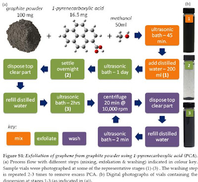
Researchers at Rensselaer Polytechnic Institute have developed a simple new method for producing large quantities of the promising nanomaterial graphene. The new technique works at room temperature, needs little processing, and paves the way for cost-effective mass production of graphene.

Posted Image

By submerging graphite in a mixture of dilute organic acid, alcohol, and water, and then exposing it to ultrasonic sound, the team discovered that the acid works as a "molecular wedge, " which separates sheets of graphene from the parent graphite. The process results in the creation of large quantities of undamaged, high-quality graphene dispersed in water. Kar and team then used the graphene to build chemical sensors and ultracapacitors

We present a scalable and facile technique for noncovalent functionalization of graphene with 1-pyrenecarboxylic acid that exfoliates single-, few-, and multilayered graphene flakes into stable aqueous dispersions. The exfoliation mechanism is established using stringent control experiments and detailed characterization steps. Using the exfoliated graphene, we demonstrate highly sensitive and selective conductometric sensors (whose resistance rapidly changes >10000% in saturated ethanol vapor), and ultracapacitors with extremely high specific capacitance (120 F/g), power density (105 kW/kg), and energy density (9.2 Wh/kg).


http://news.rpi.edu/...tcenterkey=2742

http://pubs.acs.org/....1021/nl903557p

Those last two links are about the second story.
  • like x 1

#7 Reno

  • Topic Starter
  • Guest
  • 584 posts
  • 37
  • Location:Somewhere

Posted 23 June 2010 - 05:04 PM

Since researchers can now make etchable waffers with this stuff, I really wonder how long it will take them to create graphine based electronics. If it conducts electricity as it says there should be a direct and noticeable bump in computer performance in the next couple of years.
  • like x 1

#8 valkyrie_ice

  • Guest
  • 837 posts
  • 142
  • Location:Monteagle, TN

Posted 23 June 2010 - 05:17 PM

Since researchers can now make etchable waffers with this stuff, I really wonder how long it will take them to create graphine based electronics. If it conducts electricity as it says there should be a direct and noticeable bump in computer performance in the next couple of years.


One does hope. IBM has already made a test circuit that ran at over 60GHz. Combine it with Tilera's massively multicore architecture (64 and 100 core chips) and we could see some MASSIVE explosions in computing power.

#9 Reno

  • Topic Starter
  • Guest
  • 584 posts
  • 37
  • Location:Somewhere

Posted 23 June 2010 - 06:34 PM

Some seem to think I'm full of it about the tech industry fixing the rate of advancement in order to milk the consumer. However, I still think we won't see those sorts of speeds for awhile. There is just too much money to be made in puttering along.

It would be nice though. AI would be a hop, jump, and skip away with those sorts of speeds.

Edited by Reno, 23 June 2010 - 06:39 PM.


#10 valkyrie_ice

  • Guest
  • 837 posts
  • 142
  • Location:Monteagle, TN

Posted 23 June 2010 - 07:38 PM

Some seem to think I'm full of it about the tech industry fixing the rate of advancement in order to milk the consumer. However, I still think we won't see those sorts of speeds for awhile. There is just too much money to be made in puttering along.

It would be nice though. AI would be a hop, jump, and skip away with those sorts of speeds.


I've worked in the tech industry, Reno. I've seen firsthand exactly how cutthroat they are trying to outdo one another to steal market share. I worked for Sony, and the overwhelming effort they put into trying to one up the other tech companies was just plain NUTS. I'm not saying there is no chance you might be right, but I've seen no evidence to support it, and a lot of evidence contrary to it.


But speed alone won't solve the AI problem. Nor will ultrafast processors immediately mean ultrafast programs. We've lagged seriously behind hardware ability in our ability to program for massively parallel systems. Even today, we've got hardware like the Wii and Kinect which are being used as console controllers, and seriously lacking in programs which can properly utilize them, not because of hardware limits, but because they are VR controllers and we've yet to program the VR programs to use them

What ultrafast computers WILL do is allow brute force solutions to be practical for a lot of very useful narrow AI applications and VR programs.
  • like x 1

#11 Reno

  • Topic Starter
  • Guest
  • 584 posts
  • 37
  • Location:Somewhere

Posted 23 June 2010 - 07:54 PM

The Blue Brain Project project uses the IBM super computer to simulate a cat brain. I think it was something like simulating 60,000 neurons. Give it more processing power and with a little luck you'd looking at real time simulation of a human brain.

You might be right about some of the companies in the tech industry, but I'd bet the rest are worse then you think. Look at Apple and the cell phone industry. Any of the big mobile phone companies could have come out with touch screen hard drive based phones. It took a company wanting to break into the market to drag all the others to manufacture more expensive hardware. They were fine with the status quo. At least they were until another company came in and left them behind by taking advantage of the situation.

The LCD screen corporations did the same thing by creating an industry wide price fixing cartel.

http://www.pcworld.c...ricefixing.html

Edited by Reno, 23 June 2010 - 07:59 PM.


#12 valkyrie_ice

  • Guest
  • 837 posts
  • 142
  • Location:Monteagle, TN

Posted 23 June 2010 - 08:58 PM

The Blue Brain Project project uses the IBM super computer to simulate a cat brain. I think it was something like simulating 60,000 neurons. Give it more processing power and with a little luck you'd looking at real time simulation of a human brain.

You might be right about some of the companies in the tech industry, but I'd bet the rest are worse then you think. Look at Apple and the cell phone industry. Any of the big mobile phone companies could have come out with touch screen hard drive based phones. It took a company wanting to break into the market to drag all the others to manufacture more expensive hardware. They were fine with the status quo. At least they were until another company came in and left them behind by taking advantage of the situation.

The LCD screen corporations did the same thing by creating an industry wide price fixing cartel.

http://www.pcworld.c...ricefixing.html


You kind of make my point for me, Reno. It doesn't matter if a group tries to "control the market" because there will ALWAYS be that "someone looking to break into the market" who will be willing to cut their throats while giggling.


Do you seriously think GOOGLE had any real intent to become a major cellphone dealer? I never did. I saw them offer a "googlephone" for one reason and one reason alone. To BREAK Apple's hold on cellphone OS.


And they did. The harder Apple tries to make a walled garden now, the more APPLE will push people towards Android.


Intel might try to "limit" speeds, they may even get AMD to go along, but I doubt they will get Nvidia to play, or Tilera, or Motorola, all of whom stand to be far more important in the future as we move away from "desktops" to handhelds. If Intel "throttles" it's speed developments, it simply insures it will be replaced faster than it is already looking like it will be.


In a word, attempts to "prevent competition" is the final tactic of a dying corporate model. "Pricefixing" LCD's merely spurred OLED development. Attempts to "limit progress" or "milk the consumer" are last ditch efforts to maintain viability, and inevitably doomed.


I've watched it happen too many times.
  • like x 1

#13 Reno

  • Topic Starter
  • Guest
  • 584 posts
  • 37
  • Location:Somewhere

Posted 23 June 2010 - 09:37 PM

Good point. But, they do slow down the market if not completely fix progress for short periods.

I'd give you a rep point for that last one if I hadn't already reached my quota. :)

Edited by Reno, 23 June 2010 - 09:38 PM.

  • like x 1

#14 valkyrie_ice

  • Guest
  • 837 posts
  • 142
  • Location:Monteagle, TN

Posted 21 July 2010 - 07:17 PM

http://www.physorg.c...s198933750.html


In the issue of Nature published on 22 July 2010, scientists led by Roman Fasel, Senior Scientist at Empa and Professor for Chemistry and Biochemistry at the University of Bern, and Klaus Müllen, Director at the Max Planck Institute for Polymer Research, describe a simple surface-based chemical method for creating such narrow ribbons without the need for cutting, in a bottom-up approach, i.e. from the basic building blocks. To achieve this, they spread specifically designed halogen-substituted monomers on gold and silver surfaces under ultrahigh vacuum conditions. These are linked to form polyphenylene chains in a first reaction step. <br style="clear: both; ">

In a second reaction step, initiated by slightly higher heating, hydrogen atoms are removed and the chains interconnected to form a planar, aromatic graphene system. This results in graphene ribbons of the thickness of a single atom that are one nanometre wide and up to 50 nm in length. The graphene ribbons are thus so narrow that they exhibit an electronic band gap and therefore, as is the case with silicon, possess switching properties - a first and important step for the shift from silicon microelectronics to graphene nanoelectronics. And if this wasn't enough, graphene ribbons with different spatial structures (either straight lines or with zig-zag shapes) are created, depending on which molecular monomers the scientists used.


And yet another step towards THz graphene computers. How many does that make just this year alone?


#15 Reno

  • Topic Starter
  • Guest
  • 584 posts
  • 37
  • Location:Somewhere

Posted 21 December 2010 - 06:22 AM

And the solution to recharging electric cars within minutes emerges.

Graphene supercapacitor breaks storage record

Posted Image
Researchers in the US have made a graphene-based supercapacitor that can store as much energy per unit mass as nickel metal hydride batteries - but unlike batteries, it can be charged or discharged in just minutes or even seconds. The new device has a specific energy density of 85.6 Wh/kg at room temperature and 136 Wh/kg at 80 °C. These are the highest ever values for "electric double layer" supercapacitors based on carbon nanomaterials.

The new device was made by Bor Jang of US-based Nanotek Instruments and colleagues. It has electrodes made of graphene mixed with 5wt% Super P (an acetylene black that acts as a conductive additive) and 10wt% PTFE binder. A sheet of carbon just one atom thick, graphene is a very good electrical conductor as well as being extremely strong and flexible.
The researchers coat the resulting slurry onto the surface of a current collector and assemble coin-sized capacitors in a glove box. The energy density values of the supercapacitor are comparable to that of nickel metal hydride batteries. "This new technology makes for an energy storage device that stores nearly as much energy as in a battery but which can be recharged in seconds or minutes," Jang explained. "We believe that this is truly a breakthrough in energy technology." The device might be used to recharge mobile phones, digital cameras and micro-EVs, he adds.


The team, which includes scientists from Angstron Materials in the US and Dalian University of Technology in China, are now working hard to further improve the energy density of the device. "Our goal is to make a supercapacitor that stores as much energy as the best lithium-ion batteries (for the same weight) but which can still be recharged in less than two minutes," said Jang.

His team first discovered that graphene could be used as a supercapacitor electrode material in 2006. Since then, scientists around the world have made great strides in improving the specific capacitance of these electrodes but the devices still fall short of the theoretical capacitance values of 550 F/g.

"Despite the theoretically high specific surface area of single-layer graphene (which can reach up to 2.675 m2/g), a supercapacitance of 550 F/g has not been reached in a real device because the graphene sheets tend to re-stack together," explained Jang. "We are trying to overcome this problem by developing a strategy that prevents the graphene sheets from sticking to each other face-to-face. This can be achieved if curved graphene sheets are used instead of flat ones."


source

Edited by Reno, 21 December 2010 - 06:23 AM.


#16 mikeinnaples

  • Guest
  • 1,907 posts
  • 296
  • Location:Florida

Posted 21 December 2010 - 02:45 PM

Discharged in seconds as well .....that has enormous implications in weaponry. Expect it.

#17 albedo

  • Guest
  • 2,063 posts
  • 732
  • Location:Europe
  • NO

Posted 25 May 2011 - 10:34 AM

Yes graphene looks very promising. E.g. look at the 2010 recent Nobel laureates in Physics. If project is selected (2012), graphene- driven research will make a huge step with EU funding (could reach b1$ over 10 years), e.g. see EU ICT Flaghip projects.

@Reno, btw between the 6 project finalists of the EU Flagship, next to the graphene project, there is also the evolution of Blue Brain Project, aka Human Brain Project, see http://www.humanbrainproject.eu/.

Exciting times, isn'it?

#18 albedo

  • Guest
  • 2,063 posts
  • 732
  • Location:Europe
  • NO

Posted 08 February 2013 - 04:30 PM

The Graphene project is the second winner of EU $1b funding (the other winner is the Human Brain Project with equivalent funding)
http://www.graphene-...eu/GF/index.php

#19 ihatesnow

  • Guest
  • 776 posts
  • 251
  • Location:rochester new york

Posted 07 October 2013 - 01:24 AM

http://www.cnn.com/2...arch/index.html


1 user(s) are reading this topic

0 members, 1 guests, 0 anonymous users